
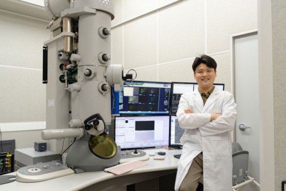
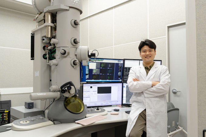
Postdoctoral researcher Cho Yong-ryun of the Advanced Analysis Center at the GIST Central Research Facilities standing in front of a transmission electron microscope (TEM). Courtesy of GIST
A method has been developed to precisely align the crystal orientation of ruthenium (Ru), a material attracting attention for use in ultra-fine interconnects in next-generation semiconductors, thereby reducing the electrical resistance of the wiring. The principle is to add and then remove trace amounts of carbon to help atoms align. When the developed technology was applied to actual nanoscale interconnects, electrical resistance decreased by 45%.
Gwangju Institute of Science and Technology (GIST) announced on the 21st that postdoctoral researcher Cho Yong-ryun of the Advanced Analysis Center at the Central Research Facilities, together with researchers from Samsung Electronics SAIT (Samsung Advanced Institute of Technology) and the Massachusetts Institute of Technology (MIT) in the United States, has developed a technique that uses trace amounts of carbon as a temporary promoter to align ruthenium crystals on a substrate. The research results were published on August 13 (local time) in the international journal Science.
In semiconductor chips, fine metal interconnects that transmit electrical signals by connecting transistor devices are densely arranged. As interconnect widths shrink to the level of a few nanometers (nm, one-billionth of a meter), ruthenium, which has excellent electrical conductivity and thermal and chemical stability, is drawing attention as a material to replace conventional copper (Cu).
Metal bulk typically exists in a polycrystalline form, composed of many “grains”—small crystalline units in which atoms are aligned in the same direction. When ruthenium is formed into a thin film, having many grain boundaries—the interfaces where grains meet—causes electron scattering, which in turn increases electrical resistance.
A key challenge in ruthenium interconnect technology is to grow individual grains to a large size, thereby reducing grain boundaries that impede electron flow, and to align the orientation of each grain in the same direction to lower resistance.
Previously, methods such as epitaxy—growing metal thin films on substrates with well-ordered crystal structures—or high-temperature annealing have been used. However, these approaches impose limitations on the choice of substrates and process conditions, making it difficult to implement them in actual semiconductor manufacturing.
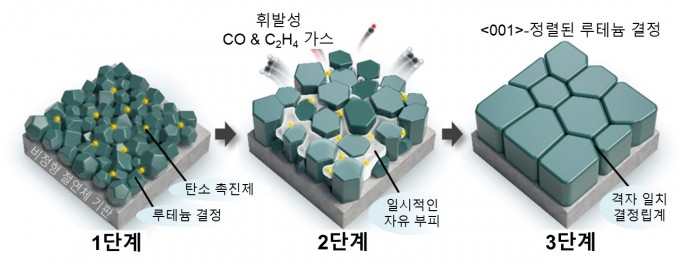
Overview of the growth of ruthenium (Ru) grains and the alignment of crystal orientation induced by the carbon promoter (C-promoter). Courtesy of GIST
The research team proposed a new strategy in which trace amounts of carbon are added to ruthenium and, as the carbon escapes during annealing, it promotes grain growth and reorientation.
During annealing, carbon atoms inside the ruthenium migrate to grain boundaries and then diffuse out, leaving behind vacant sites. These vacancies facilitate the migration of ruthenium atoms, accelerating the coalescence and growth of small grains and promoting their reorientation into similar directions.
The most effective promotion of grain growth and alignment was achieved when about five carbon atoms were added per 1,000 ruthenium atoms. Adding more carbon hindered alignment instead.
The researchers directly observed the process of grain growth and reorientation by heating samples inside a microscope using an “in situ heating transmission electron microscope (TEM).”
In experiments, the average grain size of ruthenium thin films annealed at 450 °C increased from 13 nm to 91.7 nm—about sevenfold—while the degree of crystal texture alignment, which indicates how well the grains are oriented in one direction, reached 99.3%.
The electrical performance of the ruthenium thin films also improved. In tests on 8 nm-thick ruthenium films, the use of a carbon promoter reduced resistivity by 29.0% compared with ruthenium without the promoter. When fabricated into actual ultra-fine interconnect structures, line resistance dropped by 45.4% relative to ruthenium without the carbon promoter.
The developed technology can also be applied to complex three-dimensional semiconductor structures. When 12 nm-thick ruthenium was deposited into narrow, deep trench structures with an aspect ratio of 33:1, the sidewalls and bottom of the trench were coated with high uniformity of 99.1%.
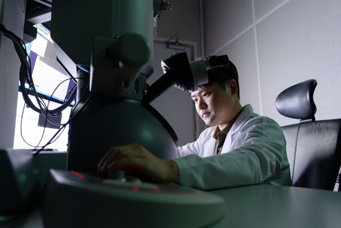
Researcher Cho analyzes and observes the microstructure of a sample using a transmission electron microscope. Courtesy of GIST
The research team explained, “This work demonstrates the potential for application to complex, highly integrated devices such as next-generation 3D memory and sub-2 nm ultra-fine semiconductor interconnects.”
This achievement is a follow-up study based on initial results obtained from an industry-academia collaboration project between the GIST Central Research Facilities and Samsung Electronics SAIT in 2024.
As a co–first author, Cho contributed to experimental design and execution, real-time microstructure analysis using transmission electron microscopy (TEM), data analysis and visualization, and interpretation of the research results.
Cho said, “We showed that trace elements in metals need not be treated as impurities that must be removed, but can instead be used as temporary promoters that guide grain migration and alignment and then diffuse out,” adding, “By tracking grain growth and reorientation during annealing, we proposed a new design principle that simultaneously controls the structure and electrical performance of next-generation semiconductor interconnect materials.”
Lim Hyun-seob, director of the GIST Central Research Facilities and professor in the Department of Chemistry, stated, “This result stems from a research culture that encourages researchers at the Central Research Facilities to freely collaborate with external teams based on their expertise and to pursue new research.”
– doi.org/10.1126/science.ady9591

From left: Dr. Lim Yong-chul of Samsung Advanced Institute of Technology, Dr. Ha Yoon-ho, researcher Lee Young-min, and Dr. Cho Yong-ryun of the Advanced Analysis Center at the GIST Central Research Facilities. Courtesy of GIST
Copyright ⓒ DongA Science. All rights reserved.